For decades, the semiconductor industry has been laser-focused on shrinking silicon transistors, but Peking University researchers believe the future might lie in changing materials entirely. In a newly published paper, the team presents a 2D gate-all-around (GAA) transistor that they claim beats the latest silicon-based designs from Intel and TSMC in both speed and energy efficiency. Built using bismuth oxyselenide (Bi₂O₂Se), a high-mobility 2D material, the transistor operates at lower voltages and could enable ultra-dense chip designs with better performance per watt.
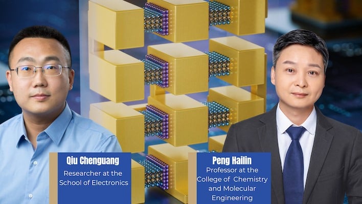
While industry giants like Intel and Samsung are working on silicon-based GAA transistors for the sub-2nm era, PKU’s researchers believe their 2D approach offers even better electrostatic control, reducing leakage and boosting efficiency. The key advantage of Bi₂O₂Se is its high electron mobility—280 cm²/Vs at these scales—allowing for 40% faster operation while consuming 10% less power than cutting-edge FinFETs. On top of that, the team has demonstrated monolithic 3D integration, stacking these transistors vertically using a layered high-K native oxide. This could solve the interconnect scaling problem that’s become a major bottleneck for Moore’s Law.

But the breakthrough isn’t just about performance—it’s also strategic. China has been locked out of extreme ultraviolet (EUV) lithography, the key technology behind the latest silicon chips, forcing domestic researchers to explore alternative pathways. Lead researcher Peng Lianhui describes it as a “changing lanes” strategy: instead of competing directly in silicon-based scaling, PKU is “exploring new material platforms that bypass the bottlenecks of traditional semiconductor manufacturing.” If this research can scale, it could help China sidestep its reliance on restricted foreign tech.
Of course, that’s a big if. The semiconductor industry is built on silicon for a reason—it’s well understood, highly optimized, and backed by decades of manufacturing infrastructure. A new material, no matter how promising, faces enormous hurdles in fabrication, integration, and yield. Just because something works in a lab doesn’t mean it will scale to millions of wafers per year. Even monolithic 3D stacking, while exciting, has long been plagued by issues like thermal dissipation and defect rates.

Still, PKU’s results suggest that 2D transistors—long sought, using other 2D materials like graphene—are no longer just theoretical. While it’s unlikely that Bi₂O₂Se will replace silicon overnight, it could find applications in low-power AI accelerators, edge computing, or ultra-dense memory architectures. If industry partners take interest—and if the fabrication challenges can be solved—this could end up being a legitimate alternative to silicon for next-generation chips.
For now, it remains an academic breakthrough, but the industry should take note. With traditional scaling getting harder and geopolitics reshaping supply chains, new materials might not just be an option—they might be a necessity.