
AMD’s new Ryzen 7 9800X3D processor has thick dummy silicon that uses 93% of the CCD stack, provides no performance benefits, and is completely non-functional, but it’s required for stability.
On previous x3D processors, the 3D chiplet was stacked on top of the CCD (Core Complex Die) which allowed the cores direct access to the pool of additional L3 cache memory, but AMD moved the 3D chiplet underneath the CCD for the new Ryzen 7 9800X3D.
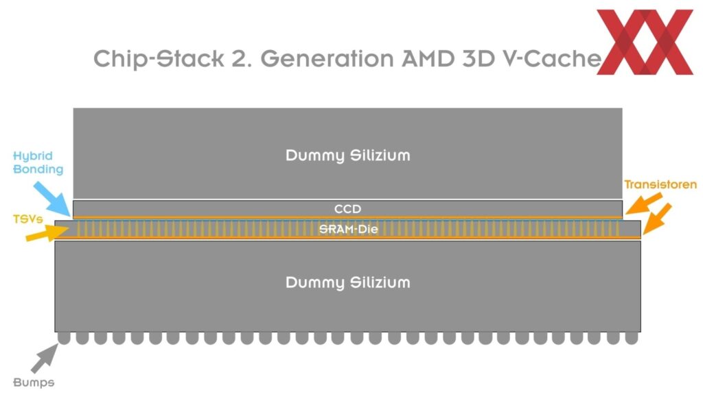
In a recent teardown of the 9800X3D, Tom Wassisk analyzed the CCD of the 9800X3D and found that most of the silicon on it is… rather useless. The CCD and SRAM silicon layers measure 7.2µm and 6µm respectively, with the total die stack and interconnects, etc measuring only 40-45µm.
The total CCD is around 800µm thick, leaving 750µm of silicon layers… the thick layer doesn’t have any functional parts, sticking to the stack in order to improve the structural support, providing more protection to that precious 9800X3D processor.
Here’s what Tom had to say:
- Both CCD and SRAM are thinned (sub 10 um), so thick dummy Si” oxide oxide bonded to the stack
- SRAM Si area is larger than the CCD — there’s a 50 um “oxide edge” for the CCD
- As with the 2nd gen, the BPV’s are terminated on the Al of the CCD
- Only saw 15 um TSV to TSV spacing in the view
- BEOL’s for the 2 die are thicker than the remaining silicon of each die
- Dummy Si oxide bond appears thinner…
- With BEOL’s included, the die stack is about 40- 45 um thick
- Total stack is close to 800, so remaining 750 is the dummy Si over the top
More findings from the 9800X3D teardown:
- SRAM Si thickness: 6 um
- CCD Si thickness: 7.2 um
- Insulator between CCD & Si slab: 425 nm, 2 distinct mat’ls
- See both 10 um & 19 um TSV pitch
- 2 um TSV drill, 1.5 um Cu diameter
- 14 level Cu + Al for SRAM
- 18 level Cu + Al for CCD